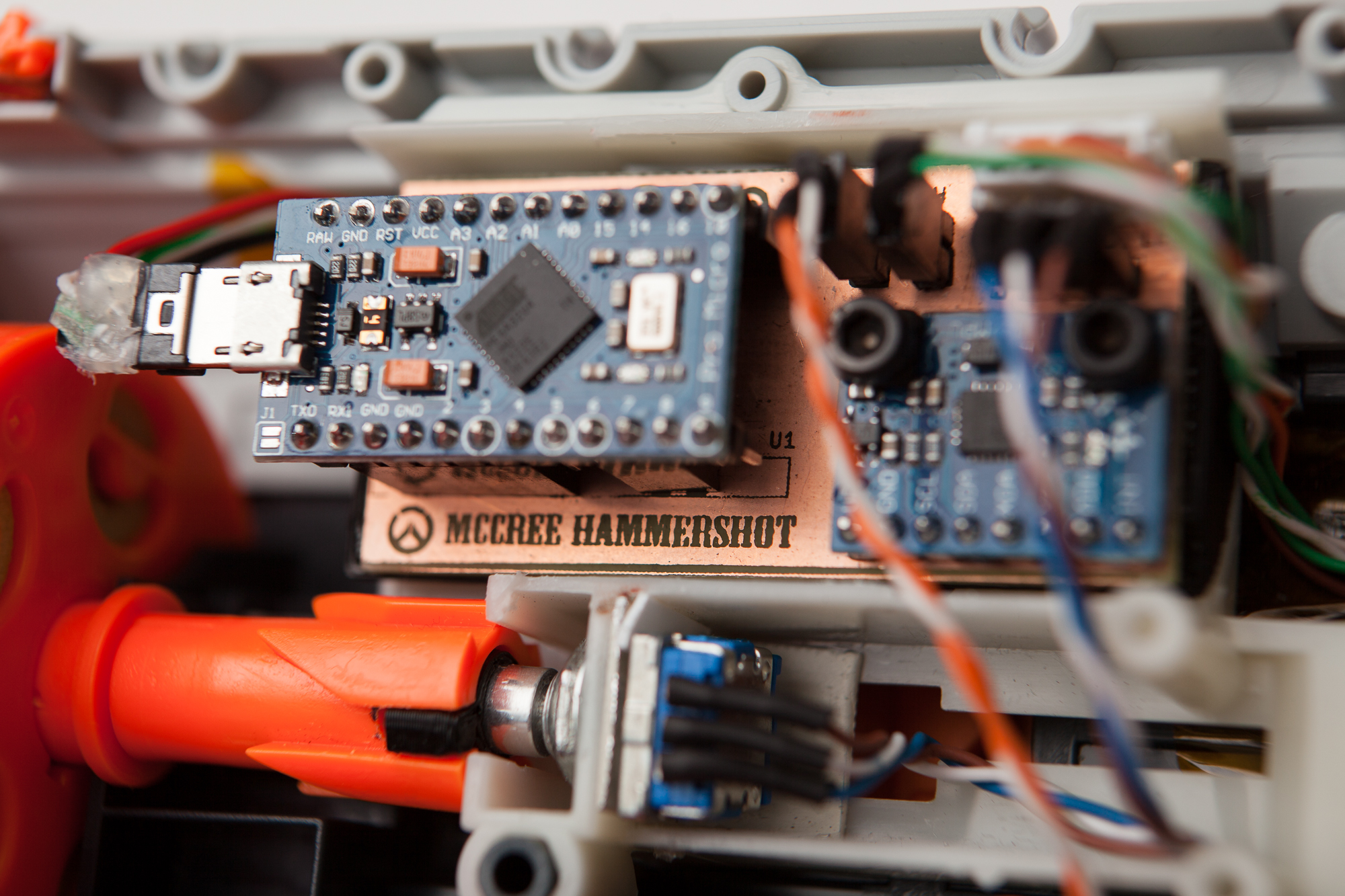
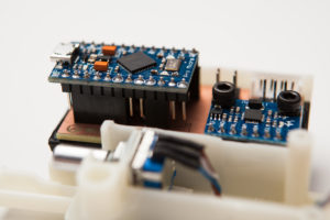
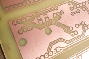
I’ve got buttons, a rotary encoder, a touch-sensitive antenna, and a fancy RGB LED. Now it’s time to tie everything together with a custom circuit board!
This post is part of a series on creating a custom controller for Overwatch using a Nerf revolver. Check out the project page here.
Planning
Let’s jump right in! There are a number of electronics around the revolver that need to talk to the microcontroller sending commands via USB. Here’s an overview of the connections:
- Trigger Button: 2 pins (Signal + Ground)
- Hammer Button: 2 pins (Signal + Ground)
- Cylinder (Rotary Encoder): 3 pins (Signal + Ground + Signal )
- Capacitive Sensor: 1 pin (Signal)
- LED: 3 pins (Power + Signal + Ground)
In addition to these, there are 3 1MΩ resistors that need to be in series for the capacitive touch sensor, and one 470 Ω resistor in series for the LED’s data line (just as a precaution).
Just Say ‘No’ to Perfboard
I wanted to put this project together quickly, and at first glance it would seem that a custom PCB would be contrary to that idea. All of the other circuit boards in the Nerf gun are just run-of-the-mill perfboard, so why not do the same for the main PCB?
From the list above there are 11 wires leaving the PCB, which for a start makes 11 custom wires that I would need to cut and place, crisscrossing, on the bottom of a piece of perfboard. Of those 11 wires, 4 of them are grounds that need to be connected together. That either means four more custom wires, or clearing a space on the board to put a single wire in a bus.
On top of the rat’s nest of wires, I also need to package all of that into a small footprint in a way that makes sense, where the connectors can easily exit in the right directions, and where I can fit mounting hardware. And after all of that, I’m still going to have a bunch of wires crossing that could short.
If I’m going to go through that much trouble to make a ‘quick’ circuit board, I’d much rather spend an extra hour or twos to make a custom circuit board that is easier, cleaner, prettier, and reproducible.
Packaging
Before I can jump into the circuit design, first I need to figure-out where the circuit board is going to sit inside of the Nerf gun.
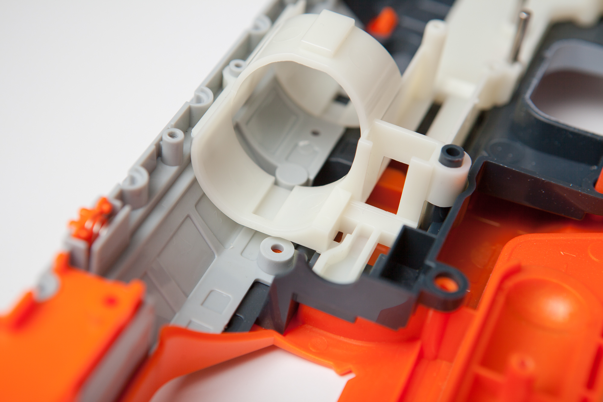
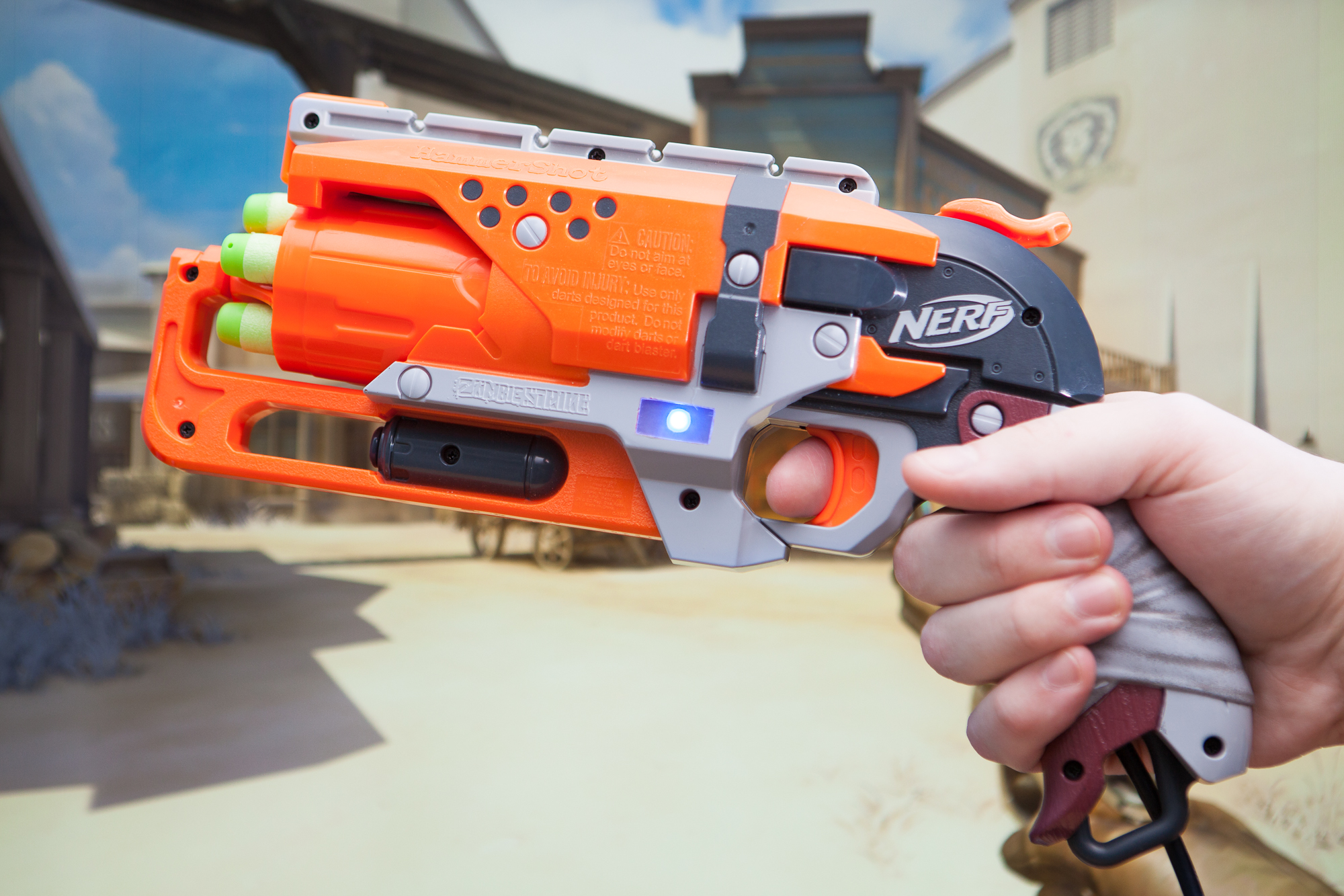
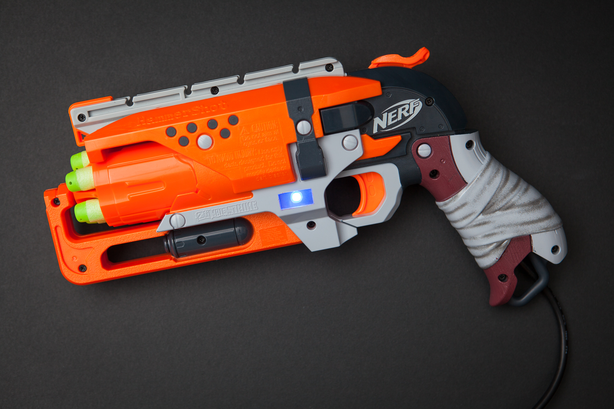
Thankfully I was thinking about this while I was working on the other parts of the gun: I’m going to put the circuit board in the nice open space where the air chamber used to sit. It’s centralized (+1 for both wiring and weight balance), removable with the white firing bracket, and large enough to fit the microcontroller and all of the connections I need.
Since the air chamber I took out is cylindrical, I will need to design a custom mount for the board, however.
PCB Design
The design pipeline for electronic design automation (EDA) software is fairly well-defined. First you make a detailed electrical schematic with all of the components and connections. Next, you match those components to physical footprints and set their positions on a virtual circuit board. Lastly, you connect everything together with traces and copper pours.
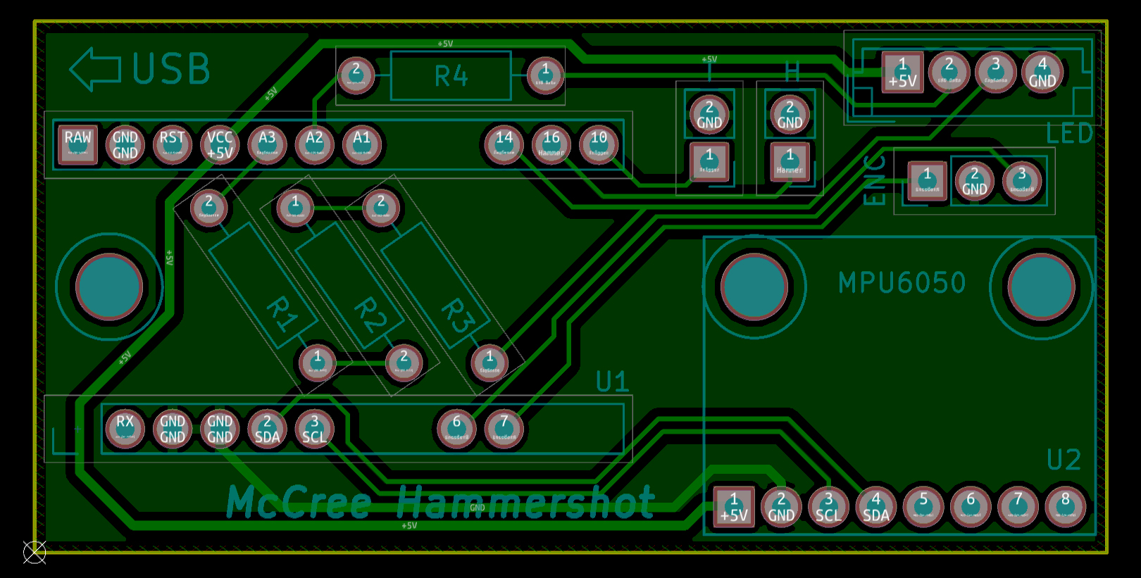
For this board I actually ended up doing this design somewhat backwards. First I figured-out where the traces needed to go, then determined the component positions, and then I put together a schematic. My software of choice for this is KiCAD, which is free and open source.
Trace Routing Limitations
Now, why am I designing this backwards? Since I’m making this at home, any holes through the board aren’t going to be plated. This means I can’t reliably use through-holes as vias without soldering on both sides, and I can’t use any vias at all unless I’m willing to drill another hole and solder a tiny bit of wire between sides (spoiler: I’m not). This leaves me with what is essentially a single-layer board, meaning that traces cannot cross each-other.
This greatly limits how I can wire everything up. On the plus side the power and I2C lines are the only connections that have dedicated pins – everything else can more-or-less connect wherever (although the encoder should go to interrupt-capable pins). It’s easier to figure-out where the simplest paths for the traces are, and then do the component placing and schematics.
If the USB port is hanging off the left side of the circuit board, the Arduino’s +5V pin (VCC) is on the top edge and the two I2C pins (2 / 3) are on the bottom edge. Both the top and bottom pin rows have dedicated grounds.
Component Positions
The air cylinder area where the PCB sits is roughly 60 x 30 mm. This is just enough room to put the Arduino Pro Micro and MPU6050 breakout board in a line with some connectors.
To start, I’m going to center the Arduino Pro Micro vertically on the board to leave space for the traces along either edge and because it has the most clearance inside of the Nerf gun (remember: it’s replacing a cylinder). And since the I2C lines need to run along the bottom edge, it only makes sense to place the MPU’s pins along the bottom edge.
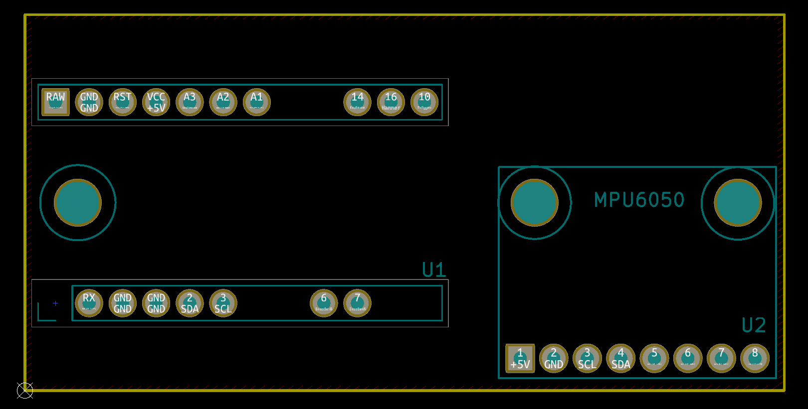
For the IMU to function as well as it can, it needs to be rigidly mounted. There are two holes through the breakout sized for M3 bolts that will do the job nicely. I centered these holes vertically on the circuit board and added a third underneath the Arduino for mounting to the frame. I’m using female headers for the Arduino so I can get to the mounting bolt underneath it (and so it can be easily replaced). The MPU on the other hand will need to be directly soldered for simplicity and rigidity.
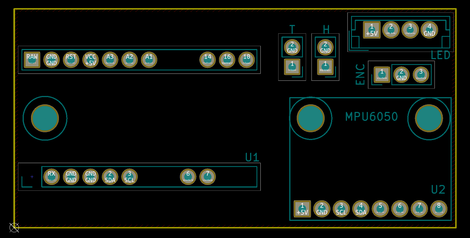
Directly above the MPU are all of the connectors. I’m using some basic DuPont connectors that are ubiquitous on hobbyist equipment – pins on the board, female connectors on the wires. For the 4-pin connector leading to the left shell of the gun I’m using a JST EH series connector shamelessly taken from my time circuits project, because it’s the only connector where polarity matters.
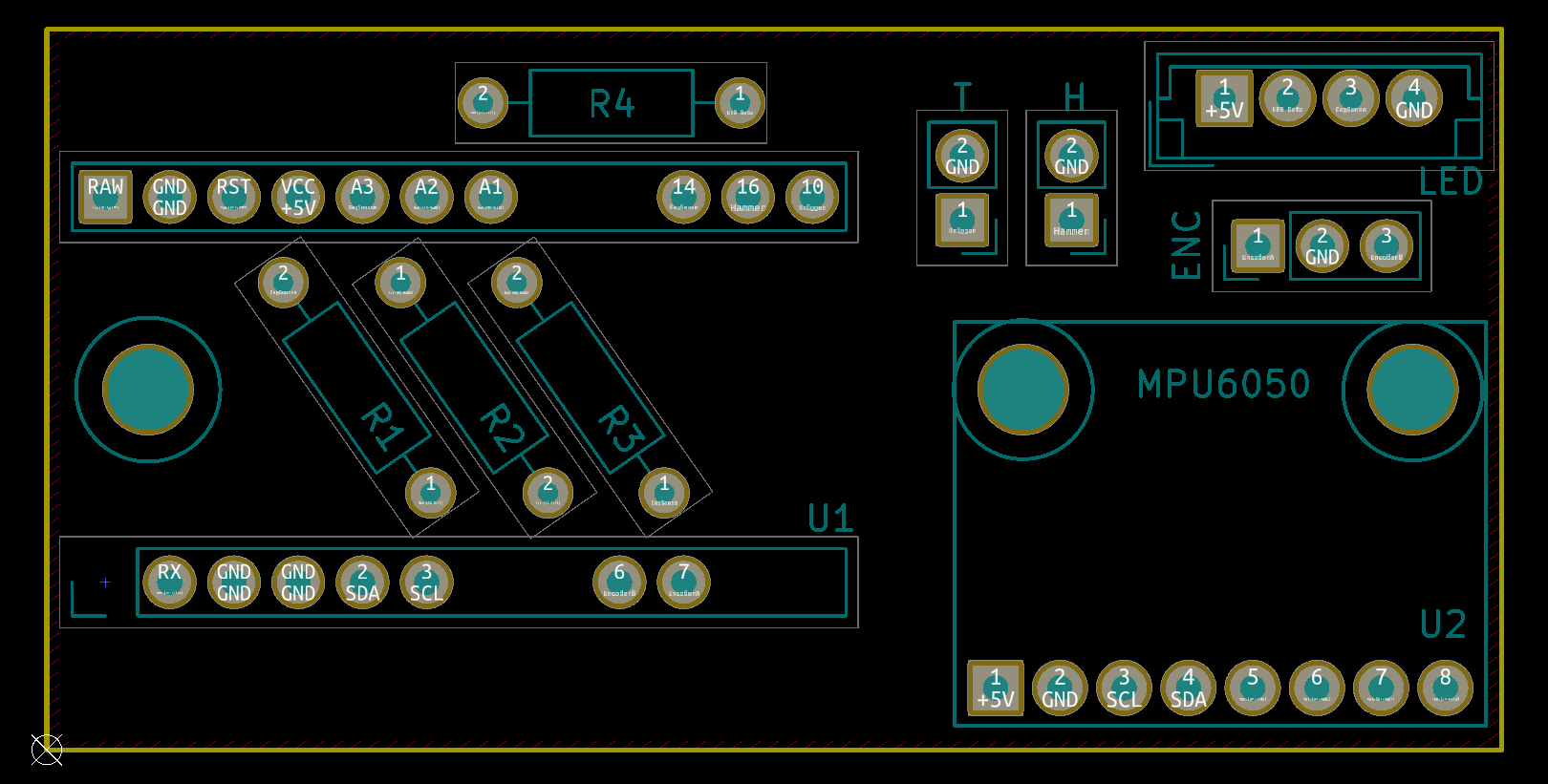
The four resistors on the board fit wherever there is space, which in this case is along the upper edge (for the LED resistor) and underneath the Arduino (for the capacitive touch resistors).
Traces and Pin Gaps
I mentioned previously that all of the connectors need to reference ground, which presents a problem for a one-layer board. The ground pins for the Arduino are on the left-most side of the circuit board, and crossing traces prevent the copper pour from reaching all of the pins.
To get around this I removed some of the Arduino’s pins from the board. The Arduino is going to be suspended in the air with some female headers, so if I remove a few pins from the board the male pins on the Arduino will just be hanging above the copper. This lets the copper pour snake its way around the board easily, and it lets me run the +5V line to the other side without a jumper.
The downsides are that I have to worry about potential misalignment when installing the Arduino, I need a few different sizes of female headers, and the board is marginally less secure. For this project the benefits outweigh those cons.
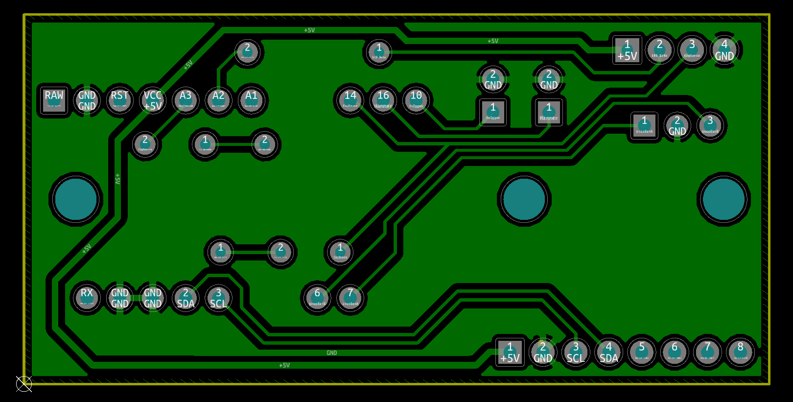
The traces were fairly straight-forward. I used 0.5 mm width on the power traces and 0.25 mm width on the signal lines. In retrospect I probably should have increased the signal trace thicknesses, just because smaller traces are harder to etch at home.
Electrical Schematic
For the schematic I made a few rough symbols and a new KiCAD library for the Arduino and breakout boards, then connected them to stock ‘connector’ symbols.
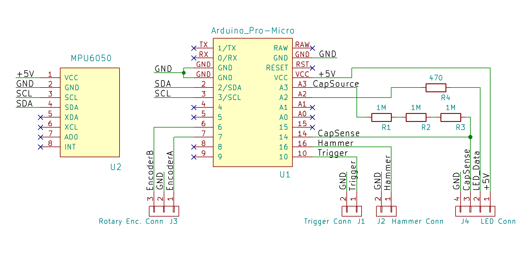
With the exception of the power and I2C pins (2 / 3) the pin assignments are dictated entirely by the trace routing. The encoder’s pin ‘A’ just happens to run to an interrupt-capable pin (7). I prototyped everything with entirely different pins and it worked fine, but this is how it works out for this board layout.
PCB Manufacturing
After a few minutes finalizing the traces and moving silkscreen items around, I had my circuit board! Now to make it.
PCB Photoshop-ing
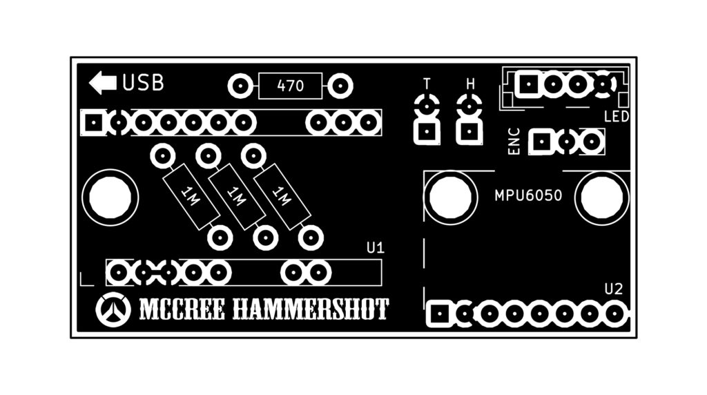
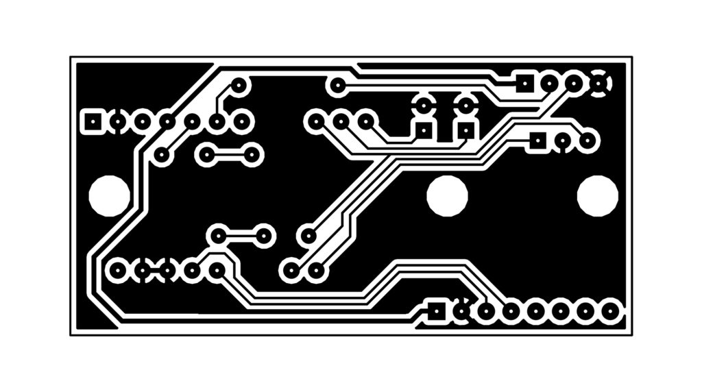
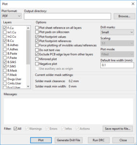
Once I was done tweaking in KiCAD I went to File-> Plot in Pcbnew and exported the circuit board layers as PDF files. I made sure to select ‘small’ drill marks, and included all of my working layers: Front/Back copper, F/B silkscreen, F/B fabrication layers, and edge cuts.
In Photoshop, I then imported one of the PDF files to set my import settings. I told Photoshop to crop to the ‘Media Box’ and imported the image at 1200 pixels per inch (PPI). This gives me a high quality image and keeps the different image layers aligned.
With those settings configured, I went to File -> Scripts -> Load Files Into Stack to import all of these PDFs as individual layers. After letting the process finish, I sorted the layers and inverted the silkscreen / fabrication layers so they’re visible on top of the black copper.
I then went through the process of turning the silkscreen into appropriate copper etching. Although all of the parts are being soldered on the bottom of the board there is a ground plane on the top copper, and I don’t want the ‘silkscreen’ I’m etching to create copper islands for the connected pins. This meant cutting little slots in the edges of the silkscreen lines to keep the copper continuous.
I also filled in the ‘USB’ arrow and spruced-up the board label with the Overwatch logo and some more… cowboy-appropriate text.

To finish it off, I added a few alignment keys and then laid out three boards for the size of my copper clad, making sure to flip the top copper so it will transfer right-side up. This sheet was then printed out 1:1 on glossy paper using a laser printer.
Toner Transfer
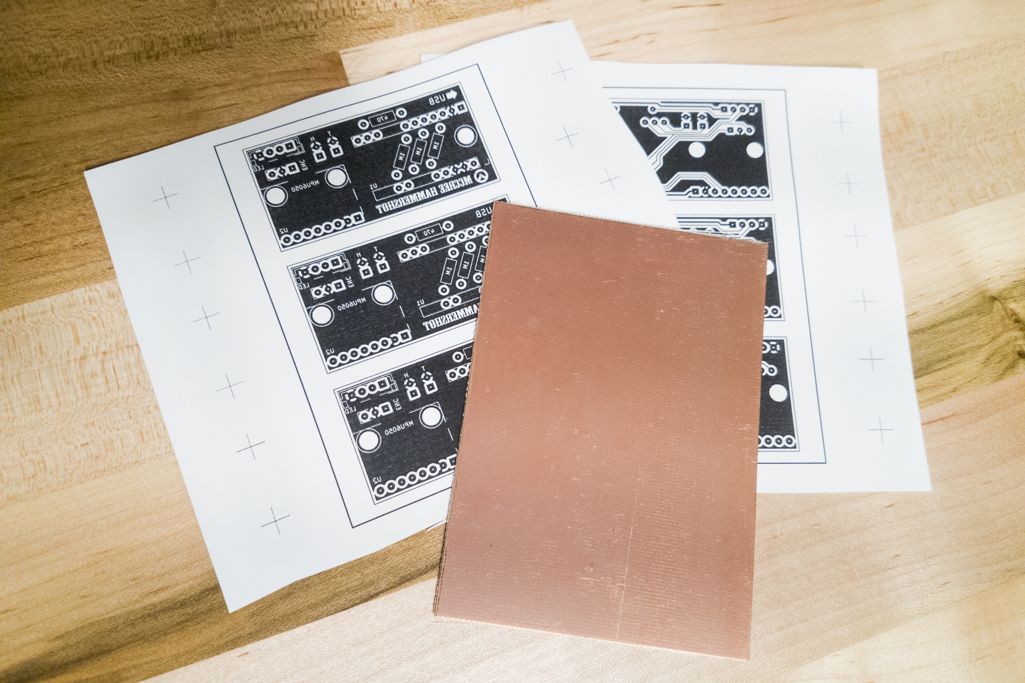
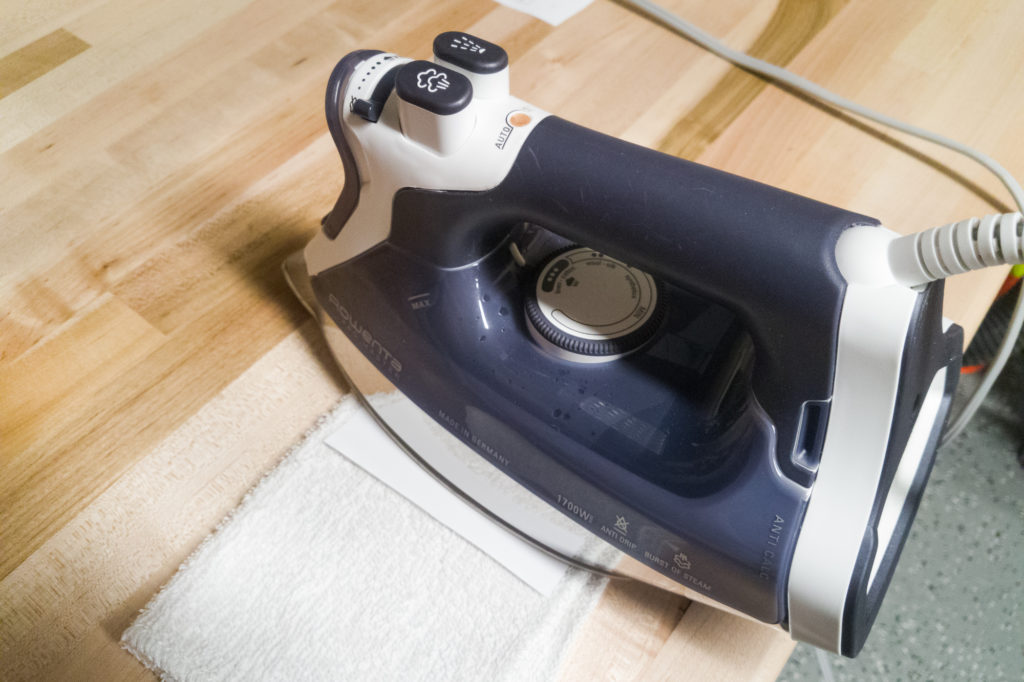
The home etching process is fairly simple. I gathered a fresh piece of copper-clad, cleaned the surface with the scouring side of a sponge, and then laid the paper with the design face-down on top. For heat, I used a clothes iron set to its highest setting (“Cotton”) with the steam setting off.
I carefully set the iron on top of the paper and left it there for a full minute to get the initial stick with the toner. After that minute I started to move the iron around, pressing firmly and trying to distribute the heat evenly. After another full minute, I then went over the entire board with the tip of the iron, paying careful attention to corners and small details. The whole side took about 6 minutes.
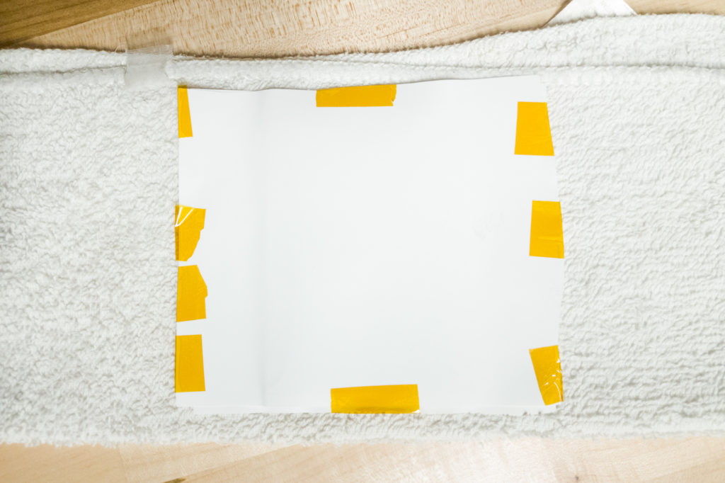
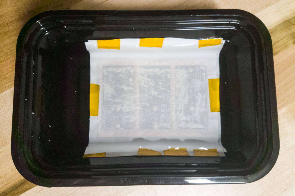
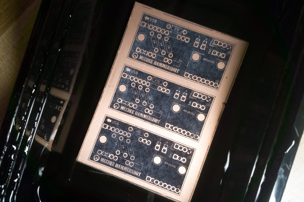
I let the board cool briefly and then flipped it over. Using the registration marks I made earlier, I lined up the other side and taped it in place using a few pieces of Kapton tape. Once it was firmly attached, I repeated the toner transfer process.
With the toner firmly attached to both sides, I put the board and paper sandwich into a tub of water and let it sit for ten minutes. After the ten minutes were up I gently pulled the paper off to reveal the toner firmly attached to the copper underneath.
Copper Etching
The copper-clad board was then put into yet another little plastic tub, this one filled with ferric chloride. Now the etching begins.
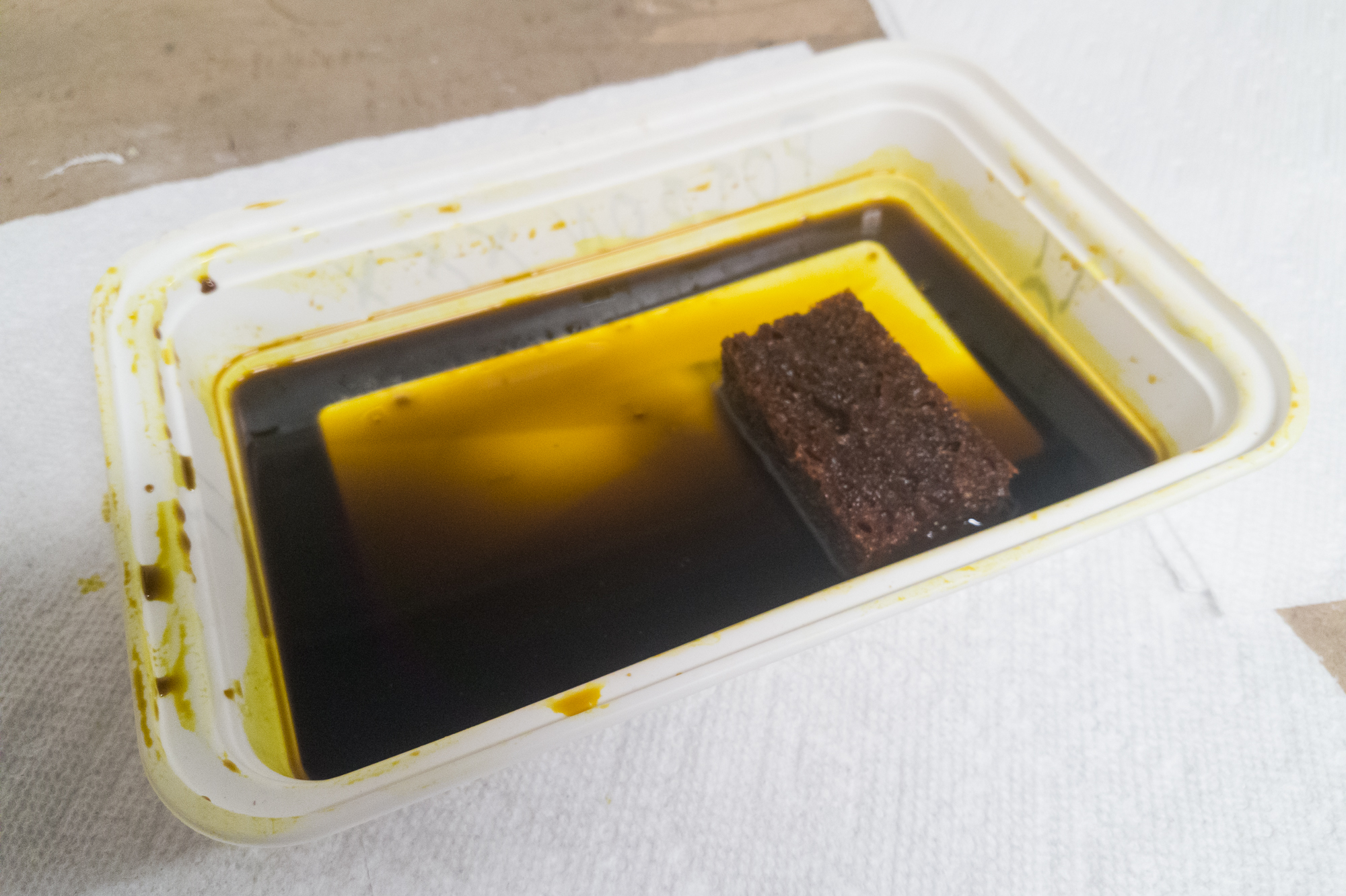
Warning: Ferric chloride is corrosive. I was wearing long sleeves, face goggles, a respirator, and using nitrile gloves. Be safe!
With a small kitchen sponge, I rubbed the etchant over top of the board. This is mostly just moving new acid on top of the metal, so there’s no reason to scrub hard. The copper comes off quickly – both sides were done in only 10 minutes.
After all of the copper was removed, I rinsed off the board and put the spent acid into a waste container. Removing the toner with a bit of acetone on a rag reveals the design cleanly etched below!
Culling and Testing
Not all of the boards made it through etching. I etched three separate circuit boards but I only need one, so I need to choose which one I like the best.
With a quick visual inspection, it’s clear that the middle board won’t do. If you look closely, one of the traces for the capacitive touch is broken. This is likely due to the toner not sticking well enough, although perhaps I was being a little too aggressive with the sponge. Either way, I could either run a wire in place of the trace or use one of my two other, un-damaged, boards.
I decided to use the bottom PCB, which looked to have the cleanest traces and the most definition for the logo on the top layer. The top board also looks good, so I’ll have a backup if I make a mistake with this one.
To check that the board was good I put my multimeter into ‘continuity’ mode and tested that the ends of all traces were connected (they were), all adjacent pins weren’t bridged (they weren’t), and that nothing accidentally connected to the ground planes that wasn’t supposed to (also good!).
Drilling, Trimming, and Soldering
When I exported the copper images from KiCAD I made sure that each pad had a small drill indicator in its center. This is important for getting the holes as close to center as reasonably possible.
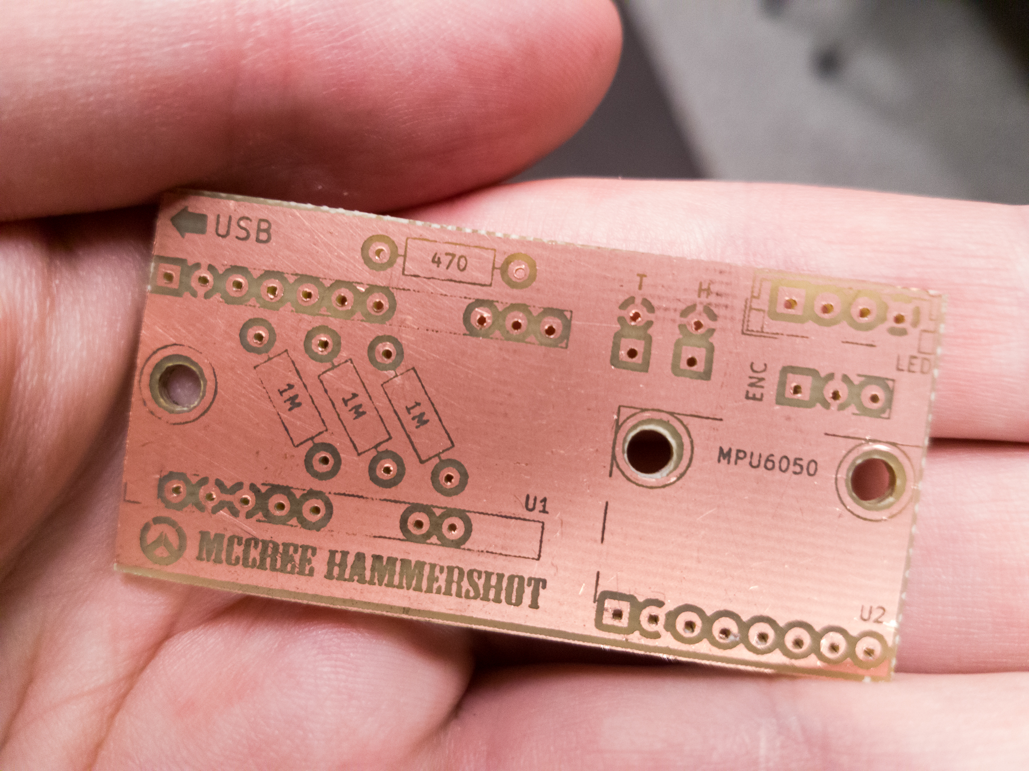
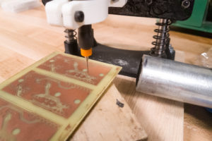
I hooked up my Dremel to my homemade PCB drill press and got to work. Each pad was first hit with a center punch and then carefully drilled out. I’ve broken far too many Chinese drill bits doing this before, so I took it slow and made sure the board didn’t shift when drilling. Still, it only took a few minutes to drill the entire board.
Warning: Fiberglass dust is nasty stuff. Wear your respirator and use a vacuum.
For cutting the board outline, I used a pair of straight-cut shears for the rough cut and then finished the edges on a belt sander. I then added the components and soldered them with some 60/40 solder on the bottom side of the PCB.
Voila! Homemade PCB!
Circuit Board Mount
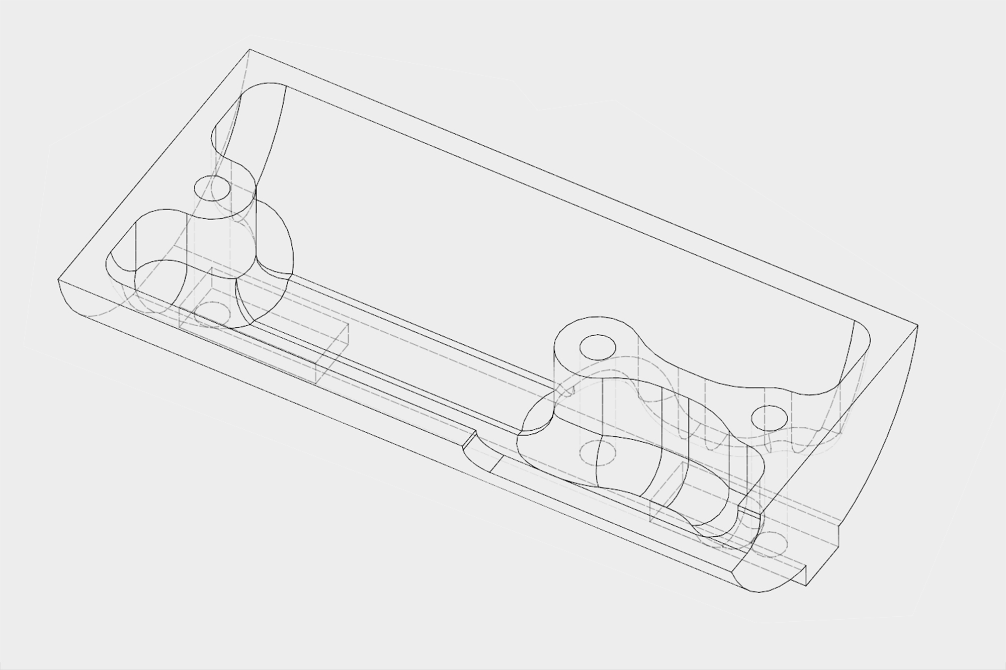
Using the air cylinder as a reference I designed a 3D-printed circuit board mount. The model has M3 mounting holes, a notch cut for the MPU6050’s pins, and locating tabs on the underside. The inside is shelled-out to allow room for solder points and any potential dead-bug circuity that may need to be added later on.
The mount took a little over an hour to print. The mounting holes were threaded with an M3 tap and the circuit board attached with a perfect fit. I used an M3-10 bolt for the mounting hole underneath the Arduino, and two M3-16 bolts for the MPU’s mounting holes (longer because of the offset height).
MPU Madness
The only component that needed a bit of coxing for the mount was the MPU6050. I used a set of male pins to solder it to the PCB, which left a small gap underneath it. I had to cut a piece of 0.118″ acrylic as a spacer, which is held in place by the mounting bolts.
Most irritatingly, the breakout board has a capacitor right underneath where the mounting bolt head rests. I didn’t have any plastic sheet of the right thickness, so I once again turned to the 3D printer to make a rough little notched standoff.
After some rough testing to confirm that the circuit board worked, I cut off the bracket’s ‘hoop’ and glued the mount in place with some cyanoacrylate glue. The circuit board can be easily swapped out or even redesigned, assuming that I keep the same mounting holes.
Conclusion
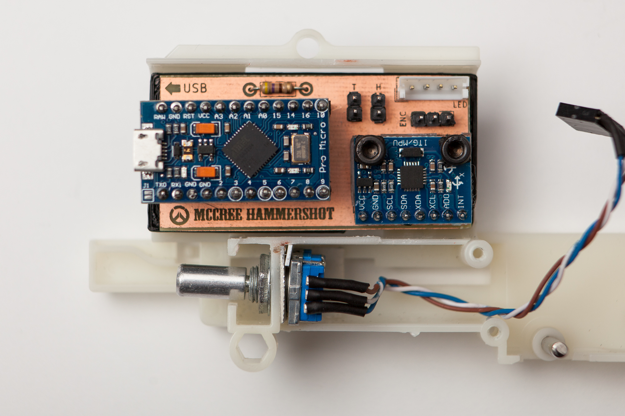
Circuit board DONE! I put this together at whirlwind pace – this post actually took longer to write than it took to design and make the circuit board.
The controller is getting so close to completion at this point. Just wiring and programming left to do!
