It’s been a long road to get to this point, but I’m finally at the stage where I can design the printed circuit board (PCB) for the time circuit display.
Footprints
In KiCAD, each respective component from the time circuit display (TCD) schematic needs a “footprint”, or its physical implementation of pads and traces on the copper of the circuit board.
SMD Components
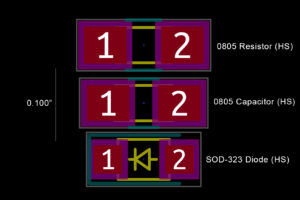
For the smaller generic components (resistors, capacitors, etc.) these footprints are already available in KiCAD’s component libraries. The only question is what package type and size to use for each component.
I’m going to go out on a limb and use SMD components for the first time. These are smaller, cheaper, and only require copper pads on one side of the circuit board. The downside is that they are significantly harder to solder by hand.
Since I am planning on soldering the entire PCB by hand, I’m going to use the 0805 package for all of these parts. It’s large enough to be solder-able by hand, and small enough to make packaging and layout of the circuit board easy. KiCAD has footprints available for 0805 resistors, capacitors, and diodes.
Kingbright Displays
There are 7-segment display footprints in KiCAD’s libraries, but I wanted to make proper-ones specific for the Kingbright displays I’m using.
The displays are through-hole components with a standard 0.1″ pitch. The 16-segment displays have 18 pins in two vertical rows spaced 0.5″ apart, while the 7-segment displays have 10 pins in two horizontal rows spaced 0.6″ apart.
For the pads themselves, I settled on a 1.8 mm pad with a 0.9 mm drill size. This is slightly smaller than the manufacturer-recommended 2.0 / 1.0 size, but should give me more room to route traces between the pins while still making solid connections. All three LED colors have the same footprint, so I can use one PCB design for all of them.
The silkscreen shows the outside edge of each display and a rough view of the segments for clarity – downsized to fit between the pins.
HT16K33
Although the 28-pin SOP package for the HT16K33 isn’t in KiCAD’s standard libraries, the datasheet lists the package’s dimensions and minimum / maximum values.
The pin pitch is nominally 0.o50″ with no tolerance listed, so the important part of the footprint to determine is the size and position of each pad. This is driven in the datasheet with three dimensions:
- ‘A’: The total width of the integrated circuit, from pin end to pin end
- ‘C’: The total width of each pin
- ‘G’: The total flat length of each pin
The width of each pad is 0.025″, which is the maximum ‘C’ value plus 0.005″ for tolerance. The 0.085″ pad length comes from a combination of the maximum ‘G’ value and both the maximum and minimum ‘A’ values. This way, the pad should be able to fit an HT16K33 chip of any size. I also added 0.020″ of length to the outside edges for solder and 0.005″ for tolerance.
PCB Layout
With all of the footprints designed and associated with their respective schematic symbols, it’s time to figure-out the layout of components on the circuit board.
LED Positions
The LED positions were already set-in-stone due to the faceplate openings, so those were positioned first. All of the LED displays were placed on the board centerline at the horizontal positions defined by the faceplate.
Mounting Holes
Next were the mounting holes. The top mounting holes were placed to re-use the mounting holes on the LMG-Heeger enclosure, and the bottom holes are mirrored about that center-line. All of the bolt holes are plated for static grounding and sized for #2 bolts (0.096″ free fit).
Board Outline
The board outline was set around the bolt holes and the enclosure spacing. The final board is 8.3″ wide and 1.475″ tall. This gives the PCB 0.025″ of clearance for its height and 0.050″ clearance for its width in the enclosure on each side.
Misc. Components
The LEDs, mounting holes, and board outline were all dictated by the faceplate and case, leaving the HT16K33 and supporting electronics to find their own place on the PCB.
The Ht16K33 is the largest and trickiest to fit. The only place on the board large enough to accommodate it was between the pins of the 7-segment displays. I ended up placing it between the ‘Day’ and ‘Year’ displays, which has the widest gap. This let me easily run the power and data traces up to a connector. The other jumpers and resistors found their place on the perimeter of the board where there is plenty of space.
Trace Routing
After placing the components it was time to route the traces to connect everything together.
Layers and Stackup
One of the first decisions regarding the trace routing was whether to go with a 2 layer or 4 layer circuit board. A 4 layer board has better shielding and makes it easier to route traces, while a 2 layer board is simpler to manufacture which means a lower cost.
Even if I decided to reposition the mounting holes, the board was already fairly large because of the LED displays. As larger boards are more expensive to manufacture I opted for the cheaper 2-layer option to keep costs down.
Trace Widths
The LED traces are neither high speed nor high power, so my trace widths were mostly dictated by manufacturing limitations. I ended up with 0.25 mm for the ‘ROW’ lines and 0.4 mm for the ‘COM’ lines, which should be plenty of copper (fingers crossed!).
The other miscellaneous traces are all 0.25 mm, and the power traces are 0.75 mm.
LED Row Traces
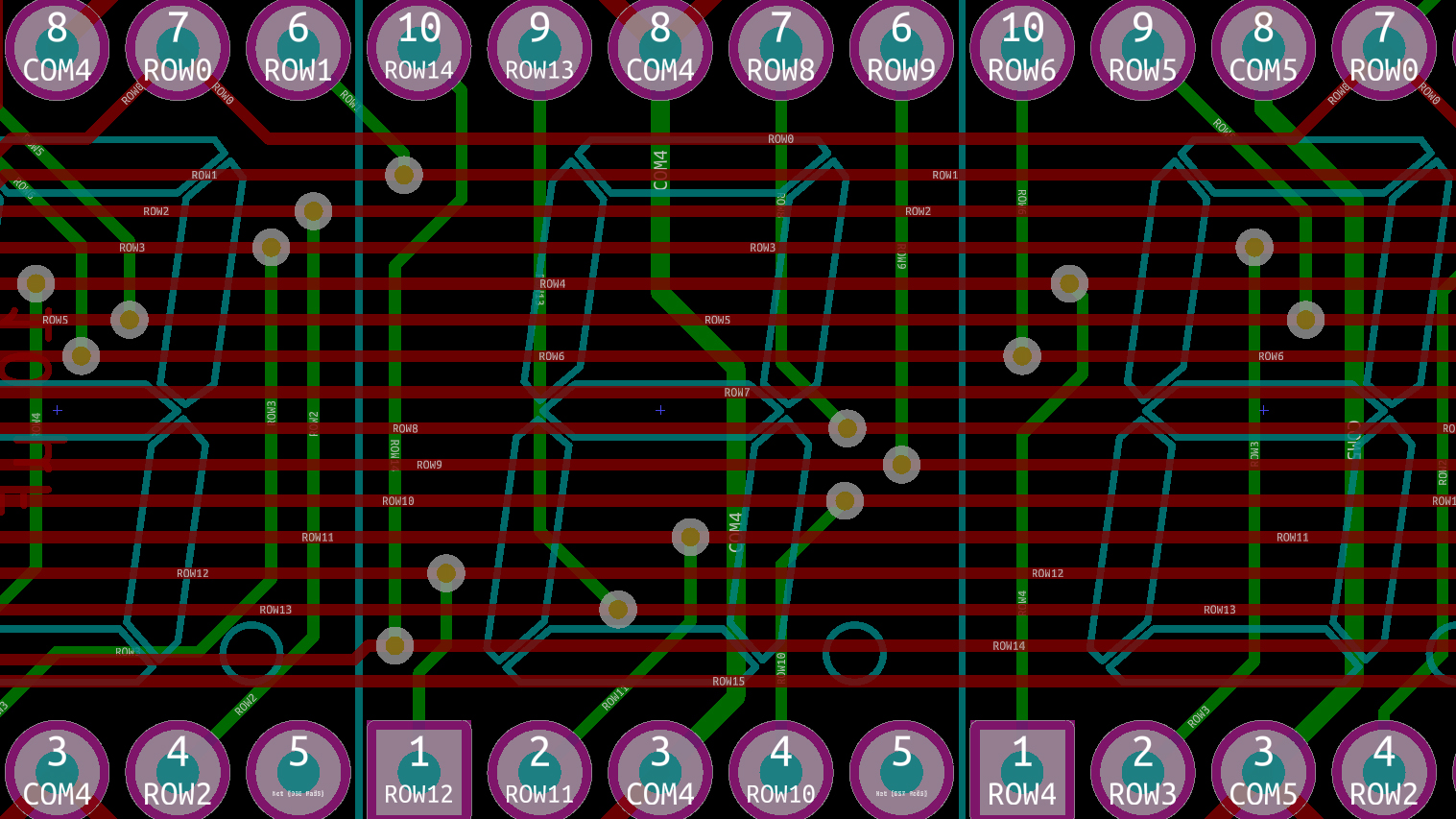
‘ROW’ traces, routed between the display pins. From top to bottom, the traces correspond to ‘ROW’ pins 0 – 15. Vias are positioned to avoid the silkscreen lines.
I started trace routing with the alphanumeric displays, which were a piece of cake since the pins are aligned vertically. But once I got to the 7-segment displays I became stuck.
I knew that I wanted to route the traces in a central ‘bus’ between the LED display pins, but I wasn’t sure how to organize the trace order. As I saw it, there were three options:
- Alphanumeric order: the same order that they come off of the alphanumeric displays.
- 7-Segment order: the order that the traces are need by the 7 segment displays.
- HT16K33 order: the order that the traces come off of the HT16K33. This is also ascending order for the row numbers.
The “alphanumeric order” was out at the start because it was a mess redirecting all of the traces to the 7 segment displays. The “7-segment” order worked much better for the first set of displays, but the traces needed to cross to get to the next set which ruined the point of putting the traces in that order in the first place.
I eventually settled on the “HT16K33” order, because the packaging for the traces gets quite complex near the integrated circuit. The downside with this is that it requires 14 vias per 7 segment display pair. This isn’t an issue because it’s well below the manufacturer’s via density limit, but it would be better and cleaner if there were fewer vias. I also organized the trace spacing to fit the vias between them which made routing and re-routing easy.
LED COM Traces and Misc.
The ‘COM’ traces were easier and routed along the outside edges of the displays. I added vertical traces along the back copper to connect both 7-segment grounds for each digit.
The rest of the traces were fairly straightforward, routed around the more complicated LED matrix traces. To finish the electrical connections I added a ground pour to both sides and a widely spaced (0.5″) via stitch around the perimeter.
3D Models and Labels
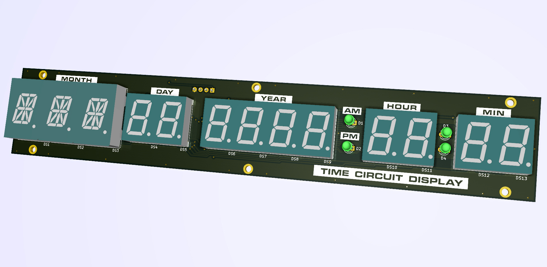
KiCAD has an awesome 3D viewer that allows you to visualize your PCB with its components in real-time. As sanity check, I added detailed 3D models to every component on the board. For the components that didn’t have 3D files available from the manufacturer I designed my own based on the datasheets.
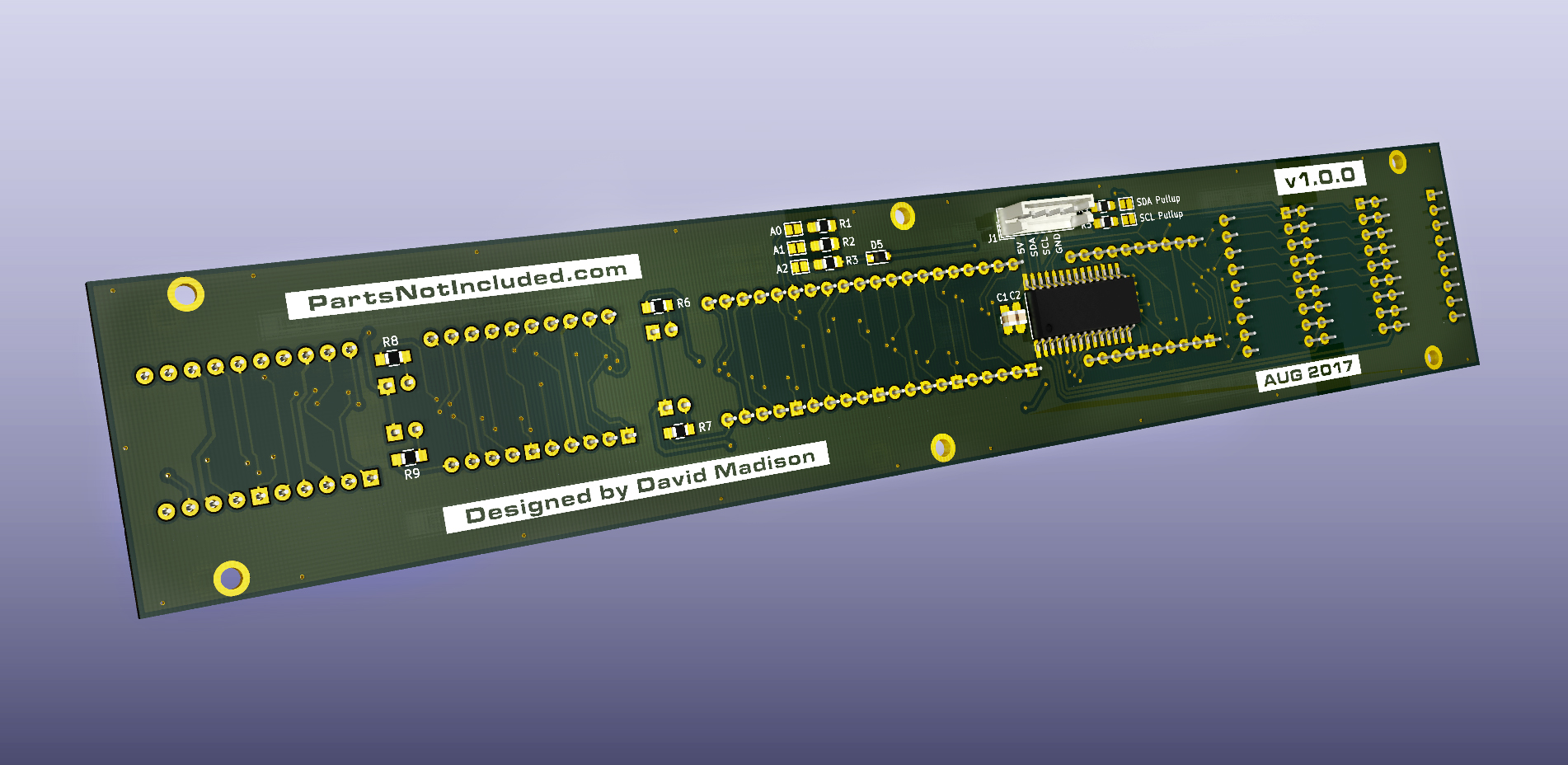
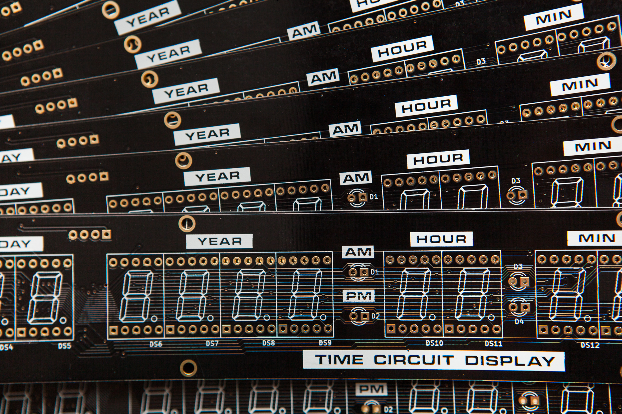
To add a bit of flash to the completed board, I designed some silkscreen labels based off of ones from the film. These were designed in Adobe Illustrator and then imported as bitmap components into KiCAD. The front of the board has the expected display labels (‘Month’, ‘Day’, etc.), while the rear of the board has the blog name and the pedigree information for the PCB.
Manufacturing
Each board has 150+ through holes for the displays and 100+ vias, so there was no way I was going through the trouble of making this at home with my little Dremel drill press. I needed to contact a PCB manufacturer.
I looked at OSH Park, which is a go-to board house for many hobbyists. They gave me a quote of $120 (!) for three boards (!!!). So I decided to look for something cheaper.
I ended up ordering my boards from DirtyPCBs.com. They quoted me $35 for 10 boards, plus $15 shipping. The website is mostly a pass-through for Chinese PCB manufacturers. Unlike most reputable PCB manufacturers there is only minimal design review and next to no communication about the status of the boards during manufacturing. From what I’ve read, the finished boards are also not particularly polished. But they are cheap, and all of the electrical connections should be solid.
I’m not worried, though. None of the tolerances on my design are particularly tight, and since the PCB is going to be marred by my mediocre soldering skill and hidden in an enclosure I don’t much care how pretty the finished board looks. So long as the electrical connections are solid and the components will mate properly, I’ll be a happy camper.
I ordered twenty boards with black solder mask and ENIG coating. If everything goes well, they should be here by the end of the month.
Conclusion
The PCB is designed and ordered! This is a huge milestone for the project, but I’m far from being finished. I still need to do the keypad and enclosure design, and design the electronics so everything can talk to each-other.
Next up: display programming


14 Comments
John · November 30, 2017 at 10:37 pm
Do you still have the KiCAD project files? Would be very interested to play with this.
Dave · December 1, 2017 at 5:21 pm
Hi John. I still have the project files but I’m not distributing them at the moment.
John · December 12, 2017 at 2:43 pm
Understandable, really appreciate the detail in your posts and have been enjoying this series – Looking forward to the next one! One question, how did you get the silkscreen of the Kingbright displays to match the outline of the actual display faces?
Dave · December 14, 2017 at 7:23 am
Thanks John, I really appreciate it.
For the silkscreen: Kingbright has CAD files for each of their displays on their website. I download the files for each display and exported the face edges into a DXF using a CAD program. After resizing the DXF in Illustrator, I then imported it as a silkscreen layer in KiCAD’s footprint editor.
Máximo Cuadros · May 12, 2018 at 7:22 pm
Hi Dave,
I wonder if you can consider distributing the project, to another Back to the Future fan!.
Tim Good · June 4, 2018 at 9:24 am
Hello Dave!
I would like to ask if you could explain how you made the 3D models of the Kingbright displays in KICAD? I am using them on a different project of mine and I’ve been trying to find a coherent explanation of how to do this but I’m not having much luck. I am quite the noob with KICAD. Did you find a good source of information on this process you could share?
Dave · June 4, 2018 at 8:29 pm
Hi Tim!
Kingbright offers CAD models of their products free to download on their website in a variety of formats, including STEP. I built this PCB using one of the beta versions of KiCAD (nightly build) with STEP file support, so it was just a matter of importing and aligning the 3D file to the footprint in either the footprint editor or Pcbnew (‘e’ -> 3D Settings -> Add 3D Shape).
Unfortunately I don’t believe STEP support is in the latest stable release (4.0.7) and I haven’t tried converting to Vrml, so I’m afraid I’m not much help there. But if you’re willing to use a less-stable version of KiCAD I found the beta STEP support to be quite easy to use.
Tim Good · June 5, 2018 at 2:34 pm
Ah well, I’ll keep trying to figure it out. Thanks for the information. If I can’t get it with the stable version, I’ll give it shot with the beta.
So anyway, it’s been quite a while since your last update on this project. Don’t keep us hanging! Have you finished it?
Dave · June 5, 2018 at 7:36 pm
Unfortunately I’ve been distracted by other things and haven’t gotten back to this. What you see on the blog is as far as I’ve gotten.
I’m getting closer to finishing my current ‘big’ project though, so hopefully with the warmer weather I can get back to the garage and working on the time circuits again.
Tim Good · June 6, 2018 at 9:49 am
That’s fine, Dave! I do the same thing, I can’t count the number of unfinished projects I have boxed up waiting for me to get back to them. I think my next project should be a clone booth so I can get another me working on them. I’ll keep checking in.
Tommy · March 4, 2019 at 8:08 pm
I’ll build mini time circuits HT16K33 version for bracelet version! But I want the same distance in seconds leds as PM & AM has & everything on a small pcb plate! My 7 segments is 0.5″
Maybe you can help me pull the wires right?? I do it in the best JLCPcb
STEPHANE · September 9, 2019 at 8:30 am
Hello Dave,
Thanks a lot for sharing so many inputs.
I want to build my own one for my daughter who is a real fan of BTTF and to make her as gift for her birthday !
To help me on this project, could it be possible for you to share the KiCAD project files? It would be very very useful.
Thanks a lot in advance
Regards
Stéphane
Frances Bent · November 30, 2019 at 9:12 am
Hey Dave, do you know what font you used for the labels? Thanks!
Dave · November 30, 2019 at 3:46 pm
Hi Frances. The font is “Microgramma Bold Extended”.